
Page 220 - 《应用声学》2024年第6期
P. 220
1396 2024 年 11 月
3.3 GaN HEMT工作波形整体测试 ination and cleaning. Oxford: William Andrew Publish-
栅极驱动正电压为 +12 V,负电压为 −3.3 V, ing, 2011: 31–62.
[2] Mishra U K, Parikh P, Wu Y F. AlGaN/GaN HEMTs-An
图 10 比较了优化前后 GaN HEMT 的工作波形,实
overview of device operation and applications[J]. Proceed-
验得到栅源极串扰电压范围从 (+2.4 V, −8.3 V) 降 ings of the IEEE, 2002, 90(6): 1022–1031.
低至 (−1.6 V, −4.4 V),振荡时间从 234 ns 减小到 [3] Lidow A, de Rooij M, Strydom J, et al. GaN transis-
50 ns;漏源极尖峰从 142 V 减小到 90 V,振荡时间 tors for efficient power conversion[M]. West Sussex: John
Wiley & Sons, 2019.
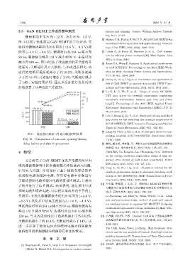
减小到124 ns。图11比较了改进前后的开关管的开 [4] Jones E A, Wang F, Ozpineci B. Application-based review
通延时、关断延时及开关损耗,与未改进前相比,改 of GaN HFETs[C]. Proceedings of the 2014 IEEE Work-
进后的电路开通损耗减小了约 10.2%,关断损耗减 shop on Wide Bandgap Power Devices and Applications,
小了约10.4%,开通延时增加了2.9%,关断延时减小 F 13–15 Oct. 2014, 2014.
[5] Huang X, Liu Z, Li Q, et al. Evaluation and application of
了 14%。实验结果证明,通过本设计进行优化后较 600 V GaN HEMT in cascode structure[J]. IEEE Trans-
好地改善了功率管的工作波形。 actions on Power Electronics, 2014, 29(5): 2453–2461.
175.31 ns [6] Lu Z, Li C, Wu H, et al. Design of active SiC MOS-
150.85 ns 160 FET gate driver for crosstalk suppression considering
120
80 t/ns impedance coordination between gate loop and power
39.49 ns
40 loop[C]. Proceedings of the 2019 IEEE Applied Power
40.64 ns
200 179.63 mJ 0 Electronics Conference and Exposition (APEC), F17–21
161.24 mJ ஈᤉҒ March 2019, 2019.
160
E/mJ 120 ஈᤉՑ [7] Liu C, Zhang Z, Liu Y, et al. Smart self-driving multilevel
87.64 mJ 78.51 mJ gate driver for fast switching and crosstalk suppression of
80
SiC MOSFETs[J]. IEEE Journal of Emerging and Selected
नᤰ Тல Topics in Power Electronics, 2020, 8(1): 442–453.
[8] Liang M, Chen J, Bai J, et al. A new gate driver for sup-
图 11 改进前后损耗与开通关断延时对比图
pressing crosstalk of SiC MOSFET[J]. Electronics, 2022,
Fig. 11 Comparison of loss and opening/closing 11(20): 3268.
delay before and after improvement [9] 陈哲, 崔龙然, 刘春强, 等. 抑制 GaN 变换器振铃的高频驱动
电路设计 [J]. 电力电子技术, 2019, 53(6): 125–127, 133.
4 结论 Chen Zhe, Cui Longran, Liu Chunqiang, et al. Research
on the voltage oscillation suppression design of high fre-
文章研究了 GaN HEMT 在兆声电源应用中出 quency drive circuit of GaN power converter[J]. Power
Electronics, 2019, 53(6): 125–127, 133.
现的栅源极桥臂串扰和漏源极尖峰振荡两大问题。
[10] Yang X, Xu M, Li Q, et al. Analytical method for RC
针对两大问题,分别设计了基于辅助电容法的串 snubber optimization design to eliminate switching oscil-
扰抑制电路和缓冲电路,在实际电路中分别进行 lations of SiC MOSFET[J]. IEEE Transactions on Power
了串扰抑制电路和缓冲电路的有效性测试,并将两 Electronics, 2022, 37(4): 4672–4684.
[11] 李小强, 林铭恩, 王文杰, 等. 抑制 SiC MOSFET 桥臂串扰
者结合进行了综合测试。结果表明,通过采用串扰
与栅源电压振荡的推挽式电容辅助电路分析及参数设计方
抑制电路和缓冲电路,可以较好地改善功率管的工 法 [J]. 高电压技术, 2023, 49(1): 226–237.
作波形,未优化前栅源极串扰电压范围为 (+2.4 V, Li Xiaoqiang, Lin Ming’en, Wang Wenjie, et al. Anal-
−8.3 V),优化后串扰电压范围为(−1.6 V, −4.4 V), ysis and parameters design method of push-pull capaci-
tor auxiliary circuit to suppress SiC MOSFET bridge-leg
串扰振荡时间由234 ns减小到50 ns,漏源极振荡尖
crosstalk and gate-source voltage oscillation[J]. High Volt-
峰由 142 V 减小为 90 V,振荡时间由 310 ns 减小到 age Engineering 2023, 49(1): 226–237.
124 ns,与未改进前相比开通损耗减小了约 10.2%, [12] 岳改丽, 向付伟, 李忠. Cascode GaN 高电子迁移率晶体管
关断损耗减小了约10.4%,关断延时减小了14%。这 高频驱动电路及损耗分析 [J]. 电工技术学报, 2021, 36(20):
4194–4203.
进一步证实了辅助电容法和缓冲电路对抑制栅源
Yue Gaili, Xiang Fuwei, Li Zhong. High-frequency drive
极桥臂串扰和漏源极尖峰振荡有显著的效果。 circuit and its loss analysis of Cascode GaN high electron
mobility transistor[J]. Transactions of China Electrotech-
参 考 文 献 nical Society, 2021, 36(20): 4194–4203.
[1] Nagarajan R, Awad S, Gopi K R. Megasonic cleaning[M] [13] 刘凤君. 现代逆变技术及应用 [M]. 北京: 电子工业出版社,
//Kohli R, Mittal K L. Developments in surface contam- 2004.